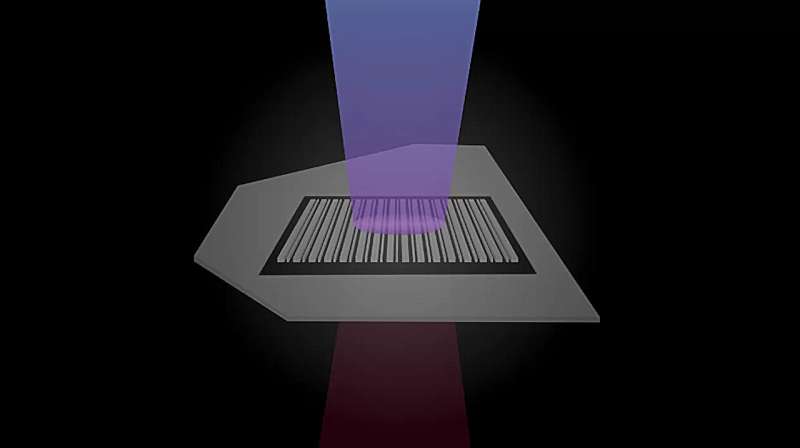
Researchers at Columbia University have made significant strides in quantum technology by developing a method to enhance nonlinear optical effects at the nanoscale. In a paper published in Nature Photonics in October, the team led by Jim Schuck successfully introduced metasurfaces—engineered geometries etched into ultrathin crystals—reducing their size to just 160 nanometers. This breakthrough could pave the way for more efficient quantum devices.
The Schuck lab focuses on a class of materials known as transition metal dichalcogenides (TMDs), which can be layered to create customizable structures. Although these materials exhibit significant nonlinear optical properties, their sub-wavelength thickness previously hindered photon generation at new frequencies. “For quantum technologies, size becomes crucial,” said Chiara Trovatello, corresponding author and assistant professor at Politecnico di Milano. She emphasized the need for smaller qubit sources to make quantum technologies scalable.
In January, the team detailed a technique involving periodic poling of molybdenum disulfide layers to optimize light output for photon generation. By alternating the direction of these layers, the researchers ensured that the light waves traveling through them would not interfere, thus enhancing the efficiency of photon production.
Innovative Metasurface Design
The latest research expanded on these concepts by focusing on metasurfaces. These artificial structures allow for the introduction of novel optical properties that do not exist in unaltered crystals. The team, including Ph.D. student and first author Zhi Hao Peng, etched repeating patterns onto molybdenum disulfide flakes to create a metasurface. “Our design enhances nonlinear effects more than traditional methods, resulting in a nearly 150-fold increase in second-harmonic generation compared to unpatterned samples,” explained Peng.
Second-harmonic generation occurs when two photons combine, producing a new photon with double the frequency and half the wavelength. With this optimization achieved, the researchers are now working on a method to reverse the process, aiming to split one photon into two entangled photons—crucial for quantum computing applications.
The technique developed by Peng simplifies the fabrication process, making it both cost-effective and efficient. “Nonlinear crystals have been essential for photonic technologies, but they are often brittle and challenging to shape,” Schuck noted. “Peng’s method is deceptively simple; we can create complex patterns using standard cleanroom etching technologies.”
Collaborative Efforts and Future Implications
The research team collaborated with theoretical experts Andrea Alu from the CUNY Advanced Science Research Center and Michele Cortufo, a former postdoctoral researcher, to determine the optimal metasurface pattern for enhancing TMDs’ nonlinear responses. “We showed that a simple modification can lead to significant improvements in performance,” Cortufo stated.
Metasurfaces have been a focus in photonics for the past decade, but this study stands out as one of the first to leverage their properties with 2D crystals effectively. Alu remarked, “This work demonstrates how engineered nonlocalities in metasurfaces can unlock unprecedented nonlinear efficiencies.”
The photons generated operate at telecommunications-range wavelengths, facilitating integration with existing networks. Schuck anticipates that this innovation could lead to one of the most compact sources of entangled photons available, enabling advancements in on-chip quantum photonics.
This research signifies a promising step towards the miniaturization of quantum technologies, potentially transforming how quantum processors and other related devices are designed and deployed in the future. With ongoing developments, the implications for both science and technology remain profound, opening new pathways for quantum innovations.


